Monday, January 28, 2013

Amazing line follower robots


Watch this space for the tutorial. Make your own line follower. subscribe to this blog.

PCB designing at home - 6

Polishing your PCB

A few drops of thinner (nail polish remover works well) on a pinch of cotton wool will remove completely the toner, bringing back the copper surface. Rinse carefully and dry with a clean cloth or kitchen paper.
Trim to final size and refine edges with sandpaper.
Finally the board is ready. You have to drill holes to place the components appropriately.

PCB designing at home - 5

Copper Etching

Next step is to remove the unwanted copper and let the copper under the toner lining remain. The board with all paper removed. It is OK if some microscopic paper fibers remain on the toner (but remove any fiber from copper), giving it a silky feeling. It is normal that these fibers turn a little white when dry. Manually examine the toner line for any breakage. in case you find any then cover it with the marker( a permanent marker)
Make a hanging tool to itch the copper. twist the plastic coated wire to make a structure as shown this will help in hanging the PCB in Ferric chloride solution(etching solution). The optimal way to etch is keeping the PCB horizontal and face-down (and possibly stirring). This way dissolved copper gets rapidly dispersed in the solution by gravity. Stirring keeps its concentration even, so the solution close to the PCB does not saturate and etching proceeds quicker.

Keep the setup immersed into the etching solution in a plastic container and let it be there for few hours.
  
 
Once complete, copper is removed leaving behind the toner lining only, take the PCB out. Rinse the board with plenty, plenty, plenty of water. Store the etching solution in the same plastic box used for etching. When the job is done put the lid on. To further minimize risks of leakage, store it in a safe place.

PCB designing at home - 4

Transferring the design

Once the clad is clean its time to transfer the printed layout to this copper clad. to do this place the paper printed paper facing the copper surface as shown below.


Iron it to transfer the print from paper to copper clad as you do it to Iron cloths. Remove the iron and let the board to cool down. You will notice the paper and the copper clad are glued to each other. Be careful not to remove the paper.
Once the board and the paper couple is cooled. Dip them in water and leave it for few minutes or five. Let the water be soaked by the paper to damage the paper so that it turns into pulp. When the board is cool enough to touch, trim excess paper and immerse in water. Let it soak for 1 minute, or until paper softens.


Cheap paper softens almost immediately, turning into a pulp that is easy to remove rubbing with your thumb. Keep rubbing until all paper dissolves (usually less than 1 minute). Don’t be afraid to scratch toner, if it has transferred correctly it forms a very strong bond with copper.

PCB designing at home - 3


Printing the design


Printing the design


The perfect paper should be: glossy, thin, and cheap. The kind of stuff that looks lustrous and shiny when new, but so cheap it quickly turns into pulp when wet. Almost any glossy magazine paper will work. I like thin paper over thick one, and prefer recycled paper over new paper.

Select the paper such that it no heavily printed, preferring pages with normal-size text on white background. Avoid printing your layout over the large text-ed Headings etc this ink may some time get on yout PCB. Cut the paper to a size suitable for your printer. Try to get straight, clean cuts, in the border otherwise it may get stuck in the printer. An office cutter is ideal, but also a blade-cutter and a steady hand work well.
Be careful to remove all staples, bindings, gadget glue or similar stuff, as they can damage printer’s drum and mechanisms.

Else you can use A4 sheets as well (it might not work always that well) Once the circuit layout is in hand take a mirror image (this is because you are going to trace this image on the copper clad similar to past and peal tattoos) print of the layout on the Magazine or simple A4 paper (glossy papers are best for this purpose).

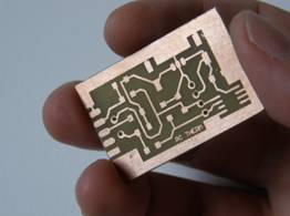
Next step is to prepare the copper clad. Cute the needed size of copper clad and rub the metal side with a kitchen scrubber or a fine sandpaper to make the surface clean and shiny. Metallic wool for kitchen cleaning purposes also works. Thoroughly scrub copper surface until really shiny. Rinse and dry with a clean cloth or kitchen paper.


PCB designing at home - 2

How do we do it.

Well the whole idea of PCB designing is to make the copper circuit. that is by keeping the necessary copper in the clad and removing the rest. There are various machine tools available do this, some are CAD tool etc. Here we are using the most simplest one is the chemical enriching technique.
The whole process can be divided into the following steps.
  1. PCB Designing or Drawing.
  2. Printing the design
  3. Transferring design to Copper clad
  4. Chemical etching
  5. Drilling
PCB Designing or Drawing

Hand made drawing  directly on the copper clad.

One of the simplest process of making a circuit manually is by drawing it in hand on the copper clad. You can use the permanent marker (CD marker is best) to do this. Use multiple repeated strokes on the clad to make the circuit line thick layer by layer. i.e. by drawing the circuit and re-drawing on the same lines so that there remains no gap within a circuit line.

                                                       Figure: Layout drawn on copper clad.

Alternative to this is a more professional and stylish way is to print the layout. For designing circuit layout you can use Eagel PCB designer. This is the software I generally prefer.


Sunday, January 27, 2013

PCB designing at home - 1

Many newbie electronic hobbies, try their luck for assembling their components with general purpose PCBs at the beginning. General purpose PCBs are good when there are less number of connection and components. Be designing becomes a challenge when the number of components and connections increases. I also did the same at the beginning which was time consuming and lessens my interest but later i switched to the home made PCB that are fare more easier to make and gives a tidy look to my artifact. Do your experiments on a bread board and deploy them on a Home made PCB. Bingo!

Drawbacks of general PCB are copper loss, heating etc. in case of radio circuit its quite noisy and needs tuning.

General purpose PCB available.

Here i will explain how you can make a PCB of your own @ home itself.

All you need is the list mentioned below.

  1. Magazines or advertising brochures (grab one from your book shelf, the paper should be shiny and glossy)
  2. Laser printer (or a permanent marker)
  3.  Household clothes iron
  4. Copper Clad
  5. Etching solution (Ferric Chloride )
  6. Kitchen scrubs
  7. Thinner
  8. Plastic coated wire