How do we do it.
Well the whole idea of PCB designing is to make the copper circuit. that is by keeping the necessary copper in the clad and removing the rest. There are various machine tools available do this, some are CAD tool etc. Here we are using the most simplest one is the chemical enriching technique.
 The whole process can be divided into the following steps.
Hand made drawing directly on the copper clad.

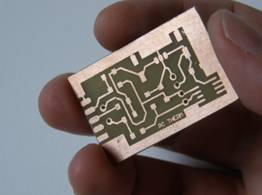
One of the simplest process of making a circuit manually is by drawing it in hand on the copper clad. You can use the permanent marker (CD marker is best) to do this. Use multiple repeated strokes on the clad to make the circuit line thick layer by layer. i.e. by drawing the circuit and re-drawing on the same lines so that there remains no gap within a circuit line.
 Figure: Layout drawn on copper clad.
Alternative to this is a more professional and stylish way is to print the layout. For designing circuit layout you can use Eagel PCB designer. This is the software I generally prefer.
Well the whole idea of PCB designing is to make the copper circuit. that is by keeping the necessary copper in the clad and removing the rest. There are various machine tools available do this, some are CAD tool etc. Here we are using the most simplest one is the chemical enriching technique.
- PCB Designing or Drawing.
- Printing the design
- Transferring design to Copper clad
- Chemical etching
- Drilling
Hand made drawing directly on the copper clad.

One of the simplest process of making a circuit manually is by drawing it in hand on the copper clad. You can use the permanent marker (CD marker is best) to do this. Use multiple repeated strokes on the clad to make the circuit line thick layer by layer. i.e. by drawing the circuit and re-drawing on the same lines so that there remains no gap within a circuit line.

Alternative to this is a more professional and stylish way is to print the layout. For designing circuit layout you can use Eagel PCB designer. This is the software I generally prefer.
No comments:
Post a Comment